Electric fields are known to have sometimes profound, and often non-linear, influences on the chemistry and microstructure evolution of solid-state materials and can be utilized to enhance processing kinetics and/or lead to highly non-equilibrium structures. While the interaction of electric fields with material kinetic processes has been of interest for many decades, there remain multiple areas where the underlying mechanisms are not completely understood.
We aim to improve our fundamental understanding of how solid materials respond to strong electric field of the microwave radiation. In particular, the electric or magnetic field of the microwave energy signifies the non-thermal effects and offers several unique capabilities for the synthesis of a variety of materials. It especially enables synthesis of non-equilibrium materials such as amorphous and amorphous-crystalline nanocomposites and synthesis of various dielectric materials at considerably lower temperatures than those of conventional routes. It is speculated that the high magnitude of the electric field can cause crystal lattice disruption and create simultaneous crystalline–amorphous phases as depicted by the schematic figure below:
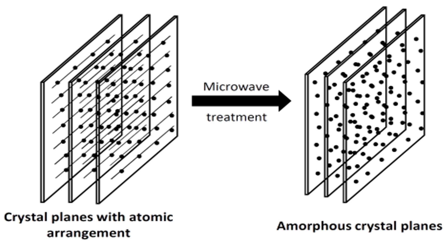
Figure 1: Schematic representation of the field induced decrystallization of the crystal planes.
Field Induced Amorphization
We have recently constructed a single transversal mode microwave cavity that provides us with an extraordinary route to create the new state of amorphous based materials in a rather quick and convenient way. The decrystallization process happens by merely subjecting the solid material to the strong E or H field in the cavity.
This unique capability opens a new landscape for discovering new electronic amorphous based structures. Since de-crystallization does not require melting of the material, the process can be scaled up for large size material processing. In our preliminary effort to determine the rate of de-crystallization in the microwave cavity, Bi doped Mg2Si powder was microwave processed at different exposure times and the crystallite size was determined by detailed X-ray diffraction analysis at each step. Figure 2 shows the result versus the exposure time.
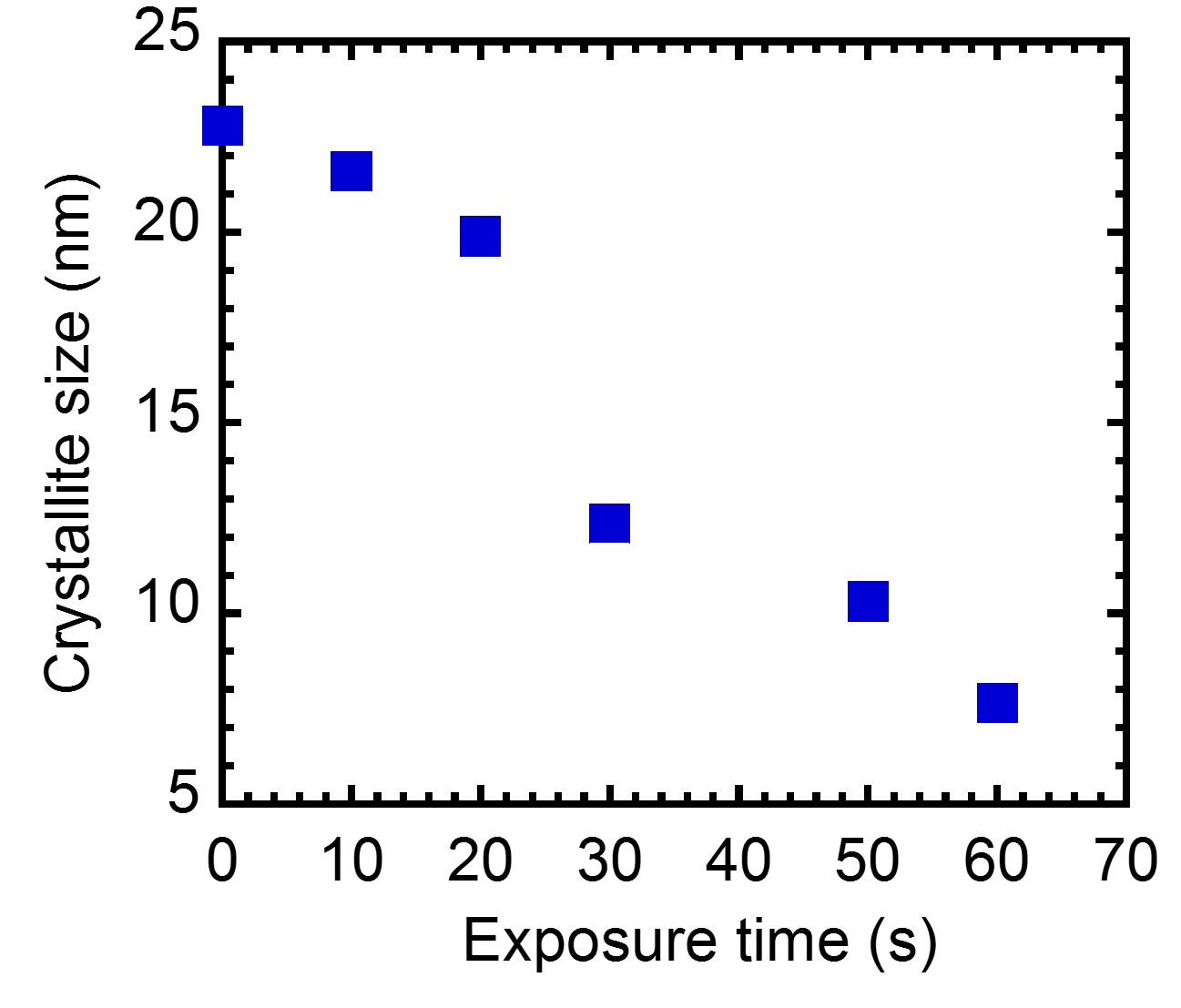
Figure 2: Crystallite size reduces rapidly with high frequency (2.5 GHz) electric field exposure.
An interesting observation and a strong subject for further investigation is the rapid drop in crystallite size by 40% when the exposure time was increased from 20 s to 30 s. With further increase of the exposure time, the de-crystallization process was enhanced and the material attained crystallite sizes of nearly 7.5 nm at 60 s. The material did not melt during this process.
In another pilot experiment, we aimed to make an amorphous SiGe alloy. In this experiment, Si and Ge powders were milled and hot pressed to form a rod of SiGe alloy (6mm diameter and 12mm long). The XRD of the powder and the hot pressed sample are shown in Figure 3. The hot pressed sample was consequently microwave processed for five minutes at sub-melting temperature in the cavity. The XRD of the microwave processed sample interestingly shows strong de-crystallization, which resulted in amorphization of the structure.
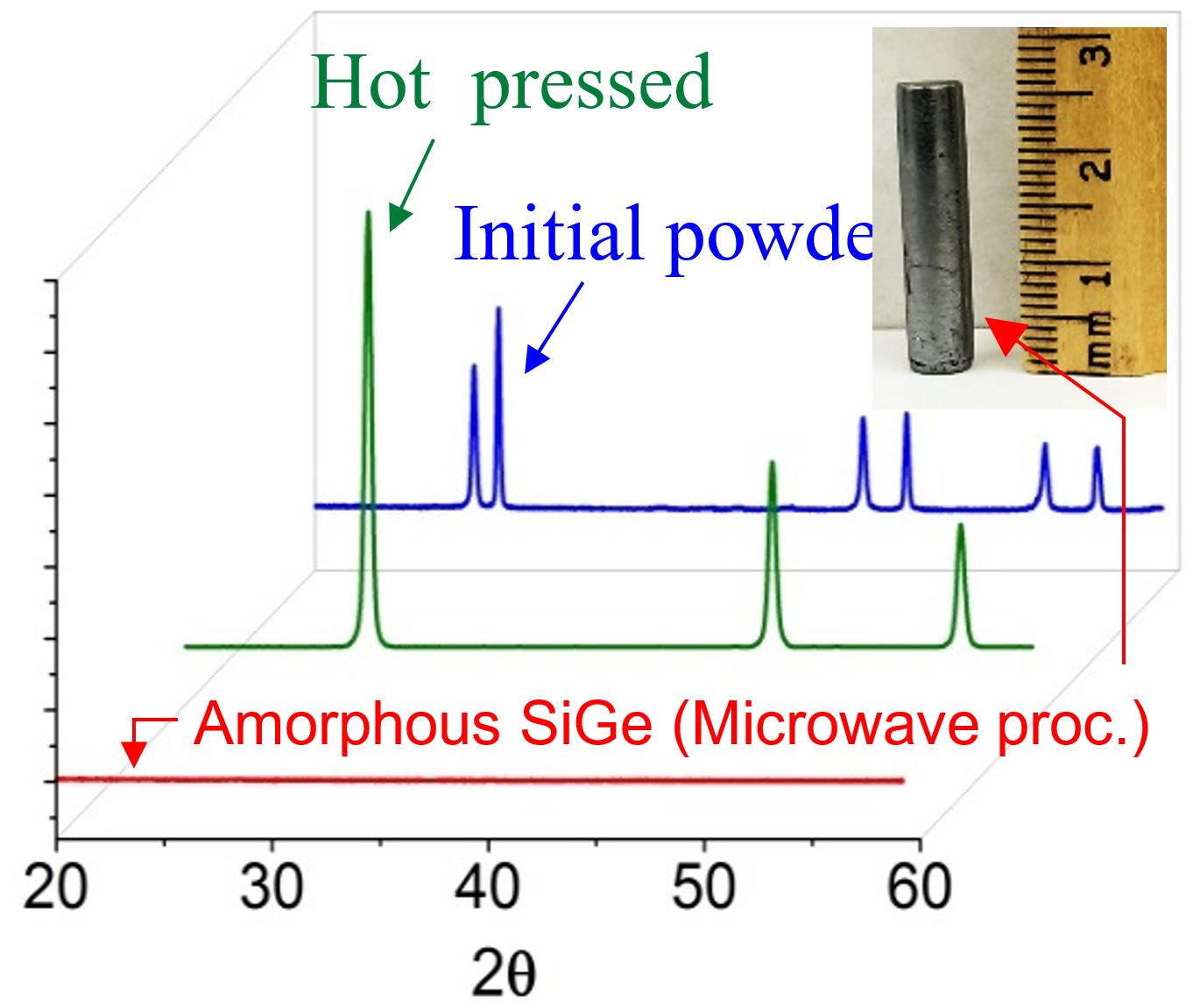
Figure 3: XRD of the Si0.8Ge0.2 microwave processed sample shows fully amorphous structure. Blue: mixed Si and Ge powder; Green: hot pressed sample; Red: microwave processed sample.
Figure 4 shows TEM image along with selected area electron diffraction (SAED) pattern of a bulk MW processed Bi2Te3 sample. The SAED pattern has the characteristic of amorphous and crystalline structure. The TEM image consists of various regions including nanoparticles and decrystallized regions. Figure 4-b illustrates STEM image demonstrating crystalline grains embedded in a decrystallized area. Initially, the whole area was decrystallized, however, while imaging a few grains were crystallized and grew. An atomic resolution TEM image (Figure 4-c) of the sample demonstrated a highly disordered/decrystallized region surrounded by crystalline grains. The region clearly reveals deviation from bulk crystalline structure.
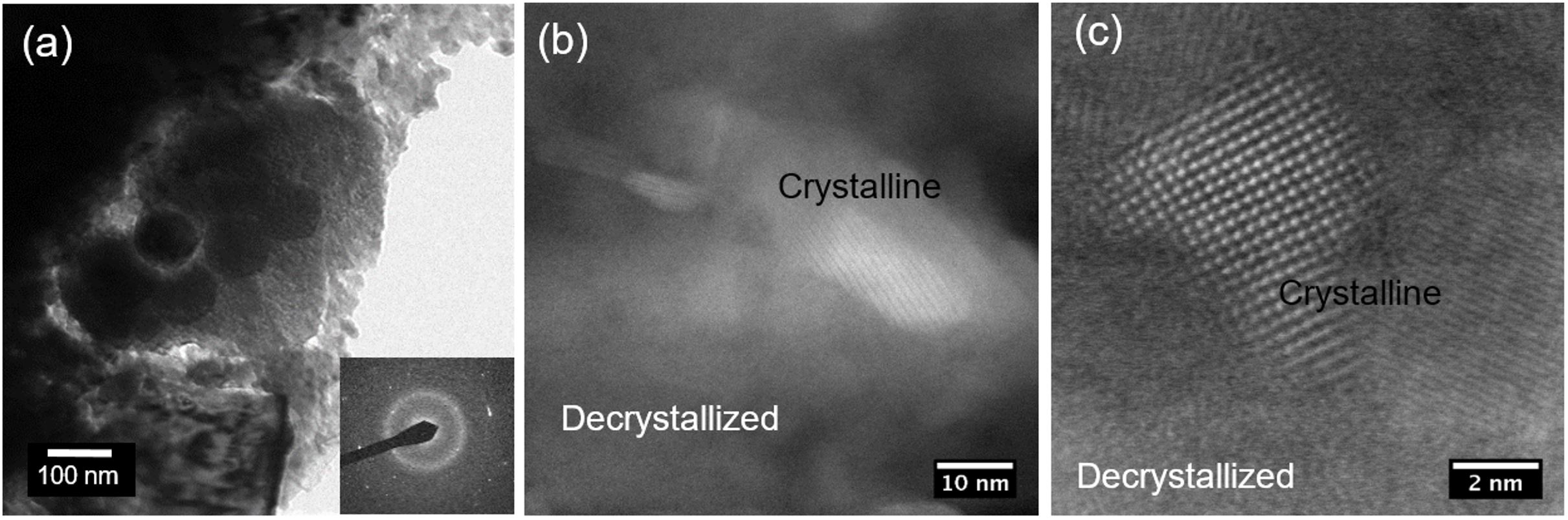
Figure 4: (a) TEM image and SAED pattern of a MW processed Bi0.5Sb1.5Te3 ingot (b) STEM image demonstrating the crystalline grains embedded in the sample, (b) higher magnification image highlighting the disordered regions present within the grains, (c) atomic resolution image of a decrystallized region with two crystalline grains.
The use of microwave (MW) energy if not only for creation of decrystallized materials. Field induced phenomena offers exciting new possibilities for the development of advanced smart materials. These possibilities are enabled by the unique characteristics of the MW processing compared to the conventional processes, namely (i) enhanced diffusion processes, (ii) decreased sintering temperatures, (iii) rapid heating rates and significantly reduced processing times, (iv) improved physical and mechanical properties, (v) simplicity, and (vii) lower environmental hazards. In addition to such unique properties, MW processing reduces the required factory floor space for kilns, and reduced energy consumption and processing cost. For example, in dental zirconia sintering, the advantages claimed for microwave sintering over traditional sintering are the following:
- Reduce sintering time by 80%
- Save up to 90% on electricity
- Create up to 20% stronger structures
Selective heating, volumetric heating, and inversion of temperature profile are some of the other unique capabilities offered by microwave processing which is not possible by conventional thermal processing methods and facilitate the development of new materials and products with desired properties.