There has been always a strong motivation for development of high-performance thermal IR detectors that operate at room temperature so they can replace photon detectors that can only operate at cryogenic temperatures. Today, the manufacturing cost of a thermal IR imaging array is still considerably high and the performance is limited by the structure of the detector and more specifically by the heat transfer between the isolated sensitive area and the surroundings. With the new discovery of enhanced thermoelectric properties of silicon nanowire, it is highly desired to use them for device application. This is especially interesting for scale up as silicon electronic devices are still the most promising one for large scale application.
Achievements
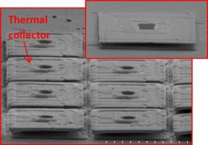
Figure 1 shows an array of silicon based thermoelectric IR detector fabricated in our lab. Micromachined Si nanowire arrays are chip scale realization of a nanostructured device. In this device, there is no need for direct metal contact to the NWs that would significantly reduce the electrical contact resistance to the wires. For this, the NWs are fabricated in parallel and in similar size off from large Silicon pads that would provide the electrical connections. Si NWs have shown a significant enhancement in power conversion efficiency (Nature, Hochbaum et al, 451, January 2008). Moreover, Si NWs are compatible with CMOS fabrication technology. This makes them ideal for chip scale integrated IR imaging.
Representative Publications
1. A Method to Measure the Thermal Conductivity of Thermoelectric Nanowires, Nahida Akhter, Daryoosh Vashaee, IEEE Green Technologies Conference 2012 – Energy Generation & Storage Technologies, Tulsa, Oklahoma, April 19-20, 2012.
2. Design Optimization of Microfabricated Thermoelectric Devices for Solar Power Generation, Lobat Tayebi, Zahra Zamanipour, Daryoosh Vashaee, Renewable Energy, 69, 166-173 (2014)
